By Paul-Henri Matha
It was a pleasure to be invited by Dr. Khasha Ghaffarzadeh to give a lecture at Techblick, explaining our DVN vision on smart surfaces for automotive interiors. Techblick gathered more than 650 experts on flexible, additive manufacturing of electronics, printed electronics, and related fields from all business areas— »GAFA » (Google, Apple, Facebook Amazon), aerospace, military, healthcare, research institute, university and automotive sectors—to share their research.
The automotive sector is a relatively tiny speck in this business, but the quantity of innovations, especially for sustainable, wearable, invisible, stretchable electronics is quite impressive and for sure this technology will proliferate in cars sooner or later, pushed strongly by the consumer/influencer sphere, GAFA, and the military.
Here’s my take on some of these forthcoming technical concepts that may apply for our automotive business. This is not an exhaustive report, which would need too much time and better expertise; me, I am just a lighting engineer!
What’s this all about?
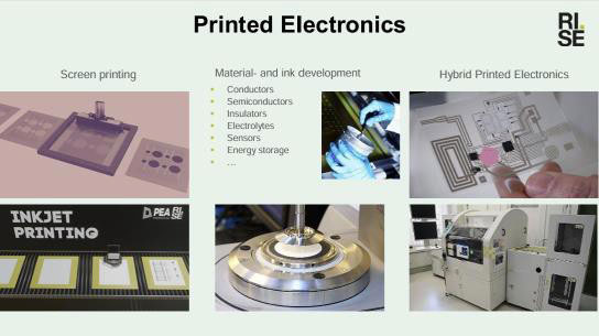
Flexible PCBs, films, and printed electronics with conductive ink involving the likes of silver or carbon.
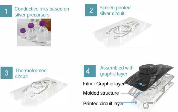

Possible military and aerospace applications
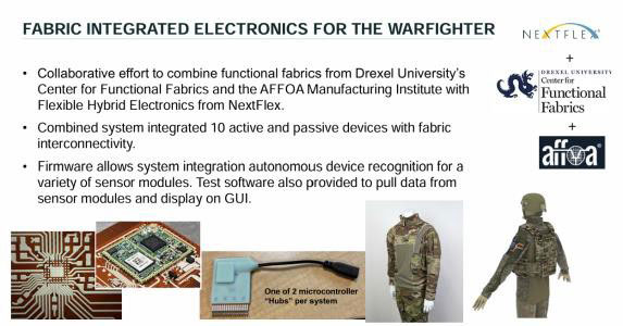
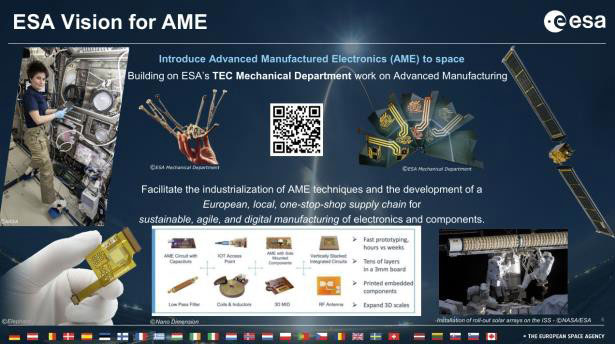
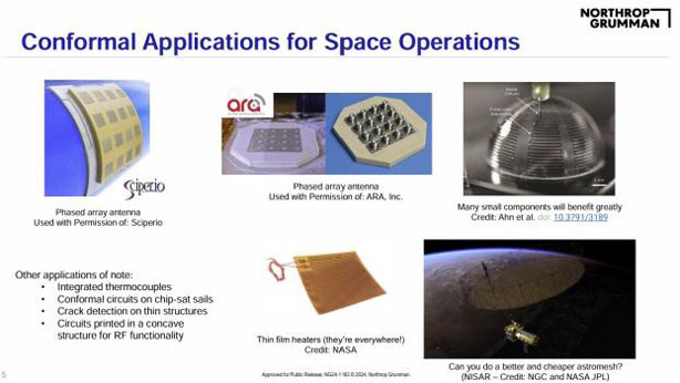
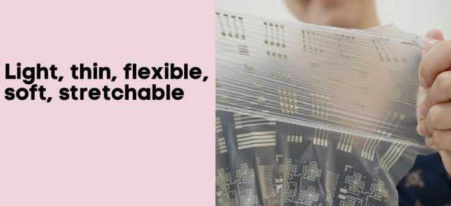
Stretchable electronics
The market for stretchable electronics is likely to grow during the next 10 years, with applications in sensor technology, healthcare, ‘smart’ textiles, soft robotics, communications, energy, and cars.
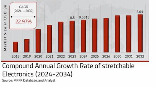
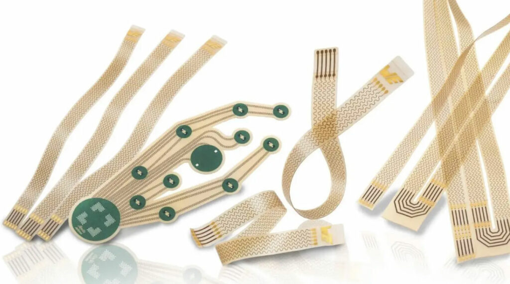
This includes stretchable printed circuit boards, with thermoplastic polyurethane (TPU) as a new copper-clad substrate material, with the tracks designed in meander form to realize the stretchability. It uses established manufacturing processes, and offers further processing options including thermoforming/deep drawing, back injection moulding, laminating, and more.


Replacement of classical FR4 PCB to reduce CO2
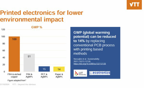
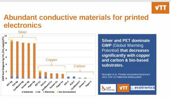
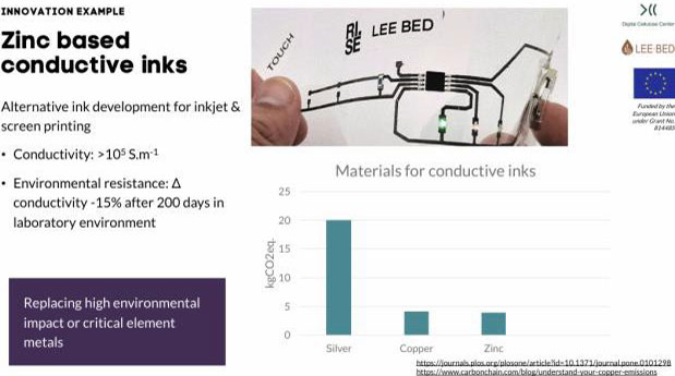
Finnish research institute VTT mentioned that global warming potential (GWP) can be slashed by 86 per cent, by replacing conventional PCB processes with printing-based methods. Similarly, usage of copper or carbon bio-based substrates for conductive material can dramatically reduce the CO2 footprint.
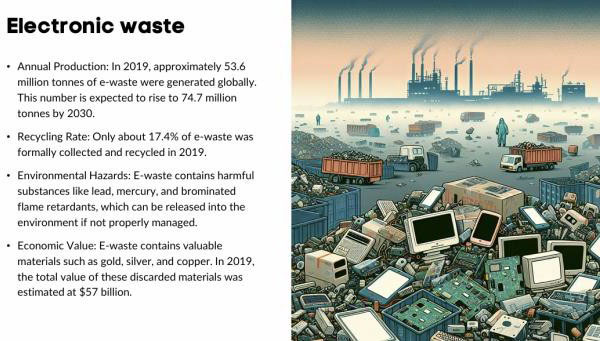
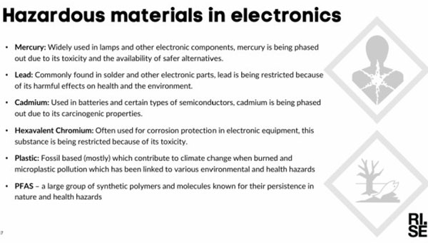
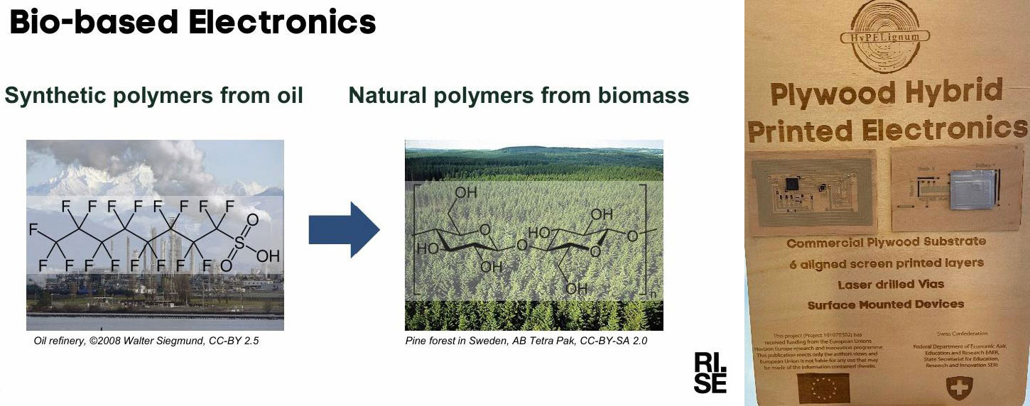
Swedish research institute RI.SE described how electronic waste (« e-waste ») is increasing from 53.6 million tons in 2019 to 75 million tons by 2030. And only 17 per cent is collected for recycling; the total lost value in 2019 is estimated at $57bn. And because of this lack of recycling, hazardous materials like mercury, lead, cadmium, chromium, and PFAS are released into the environment in massive quantities.
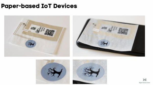
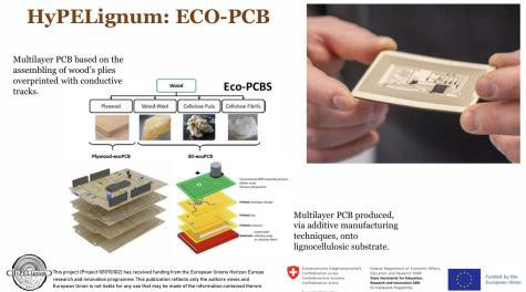
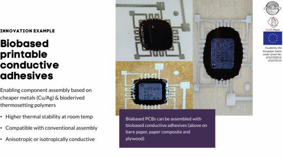
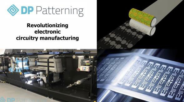
With printed electronics and especially bio-based electronics, we can tackle this problem. Solutions are ready for application.
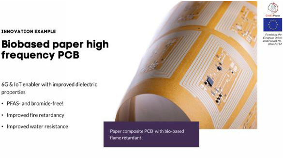
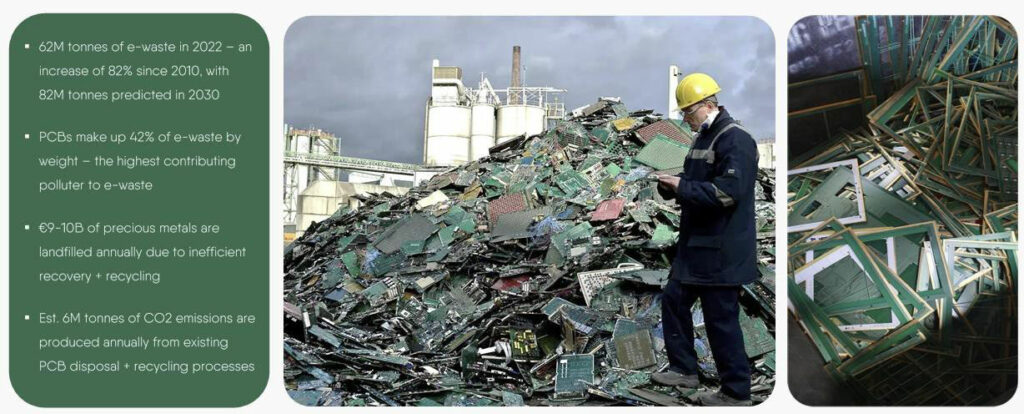
JIVA Materials showed that currently, between 40 and 60 per cent of panels become PCB waste, amounting to some €10bn. PCBs represent 42 per cent of global e-waste.
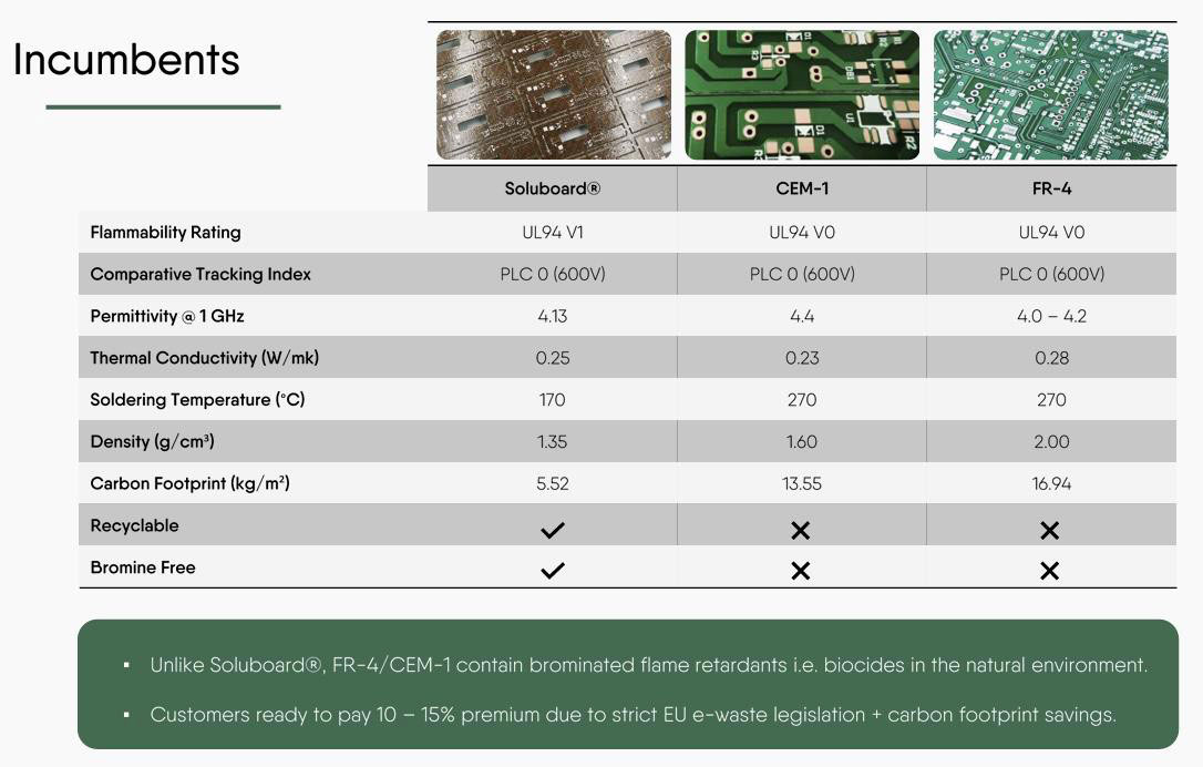
Then they presented their solution, called Soluboard: PCBs made out of natural fibres, with 67 per cent lower emissions versus FR4, and easy to recycle and re-use.


Thermal conductivity, always the main drawback with this sort of technology, has been compared and is showing good results, with performance between a CEM and FR4 PCB—a good fit for a low-power LED panel with 0.1W LED, for example.
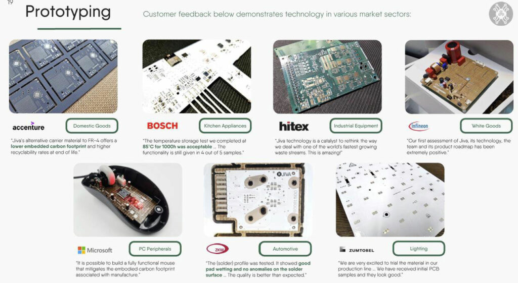
Prototypes are available and have been tested by customers like ZKW for lamp applications.
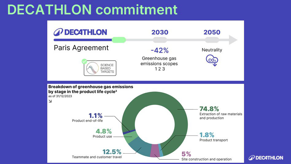
Another example of CO2 footprint reduction was presented by Decathlon, a well-known outdoor and sport article company in France. They are investigating how to redesign their production to meet their carbon footprint target with CO2 neutrality in 2050. Production is the main factor in their CO2 footprint—75 per cent.
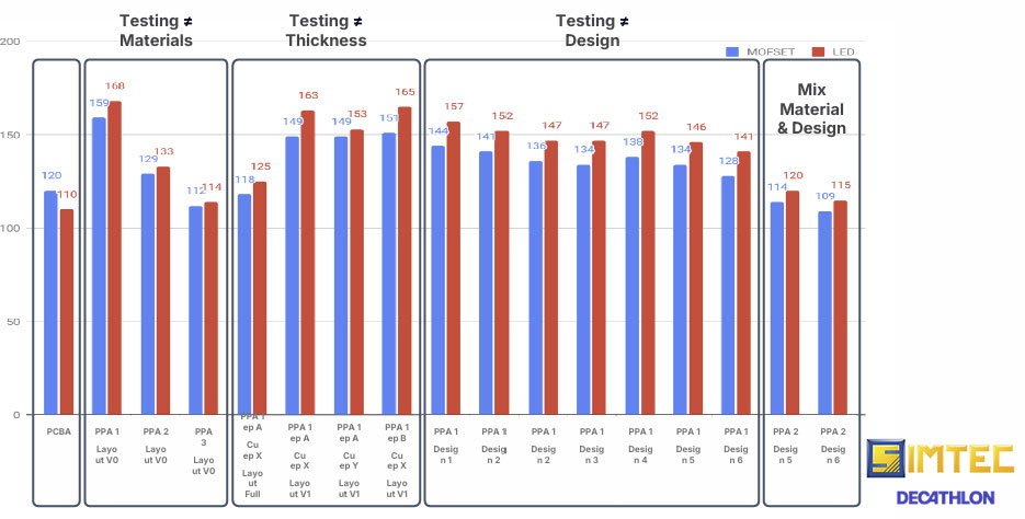
They selected as example of their LED outdoor lamp to see how printed electronics can reduce their CO2 footprint. Electronic modules account for 15 per cent of their CO2 emissions, according to their LCA (lifecycle assessment). By replacing PCBs with printed electronics, they can cut down on CO2 emissions by 20 per cent for electronic modules, and 80 per cent of the PCB material itself.

With iterative research and development, they’ve achieved very similar thermal conductivity. It’s not quite identical; the LED case temperature is up by 5 Celsius degrees, but that is judged acceptable in the application.

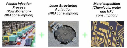
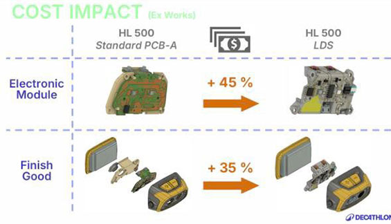
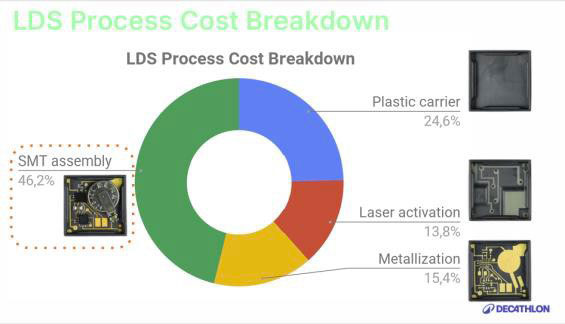
This electronic module modification raises the final-product cost by 35 per cent (SMT cost + metallization + laser ablation).
Large printed electronics
Tracxon presented additive printing on plastic foils with an SMD LED process.
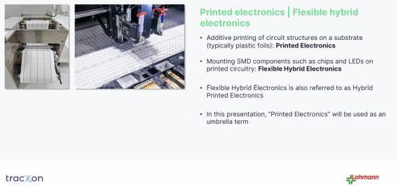
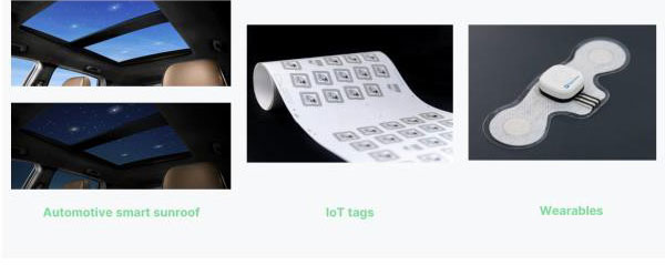
Automotive applications include sunroofs and headliners, with a fast (10 metres per minute), high-volume capacity. It’s easy to foresee, for example, an application to replace the Rolls Royce headliner with a simple film compared to the current solution with multiple hardwires and flex boards.

In-shape film
Niebling showed their technology to obtain a 3D shape from a 2D film. Film and ink elasticity properties permit to change the film shape without losing any electrical contact.

Integrated circuit for flexible PCB
French research institute CEA Leti presented their semiconductor IC that can be integrated on film without any SMD process.
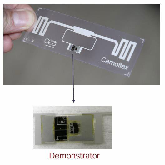
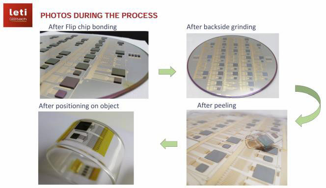
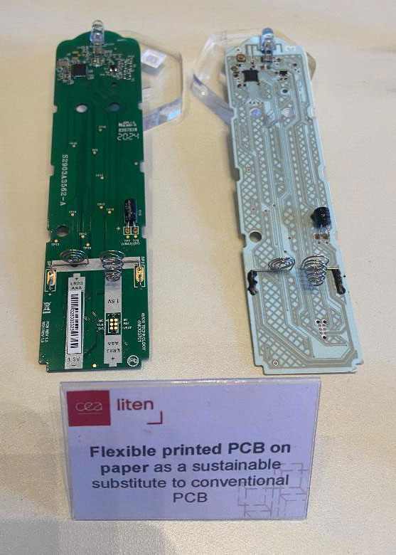
CEA Liten, another department of CEA, also showed their flexible PCB printed on paper.
3D Printed Electronics
Fuji presented possibilities to replace PCBs by additive manufacturing (3D printing) + ink deposit + SMD process.

Capillary Printing for Display Repair
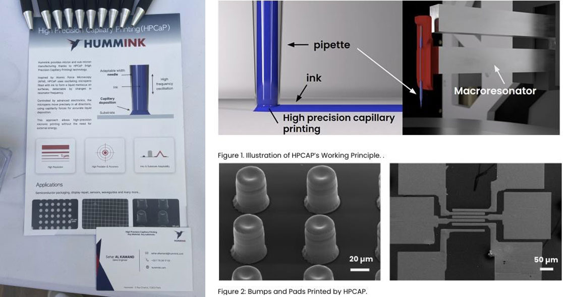
French startup Hummink showed their High Precision Capillary Printing (HPCaP) not only as a high resolution and precision printing technology, but also as a solution that minimizes material usage and actively promotes sustainability through its repair capabilities. It is inspired by atomic force microscopy (AFM), and relies solely on capillary forces for printing on substrates.
Using a macro-resonator and state-of-the-art electronics, HPCAaP achieves precise control over printing parameters, allowing adjustments in print geometry such as thickness and line width, reaching sub-micron resolutions. With a glass pipette attached to the macro-resonator, HPCaP ensures real-time interaction between the substrate and the pipette, enabling high-quality dispensing. It ensures precise and continuous ink printing with no splashes or satellite drops, and eliminates waste by using up all the materials in the pipette. HPCaP can accommodate inks in tens of microliters to produce extensive samples with minimal ink volumes. It also exhibits impressive material and substrate versatility, being able to print on recyclable substrates like paper. Remanufacturing and repair have become vital for sustainability across industries, to extend the lifespan of electronic devices, displays, semiconductors, and automotive components by preserving and reusing materials. HPCaP technology enhances repair processes in various sectors, including displays, electronics, semiconductors, and automotive. For instance, in the semiconductor industry, HPCAP addresses challenges in repairing metallization defects at the micron scale, surpassing conventional methods.
Automotive Applications
Marquardt demonstrated their printed-electronics development, begun in the early ’00s, with a keyless entry system. Similar technology is now used for diverse application like lit surface materials in door panels, and ‘smart’ surfaces including touch sensors and in-mould electronics.


Marquardt described some pros and cons of this technology—challenges like proven and cheap classic electronics or processes not being ready for this technology; opportunities like fast growing technology and supplier base, new form factors and integrations possible, sustainability through material and process savings, and possibility to increase value creation.
Forvia shared their views about ‘smart’ surfaces and printed electronics for interior application: lighting, heating and sensing.
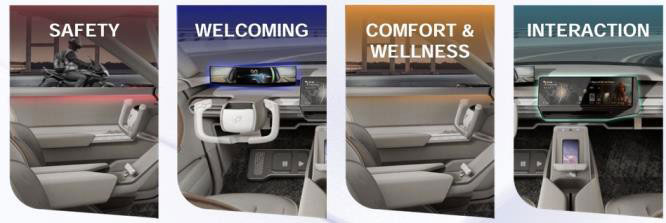
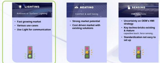
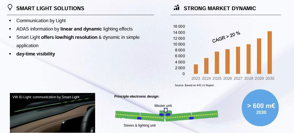
‘Smart’ lighting has a strong market dynamic with CAGR above 20 per cent by 2030.
However, similar pros and cons can be seen:
Pros: Unique pillar-to-pillar light stripes, standard and flexible solution, easy to adapt to all part designs, reduced cost to invest, develop, and integrate, compactness, light weight, and simple design.
Cons: Silver ink usage for the traces, high impedance (voltage drop with printed electronics), cost, difficulty with pick & place and electronic components, mechanical resistance on film using glue, and thermal dissipation.
The question of in-mould electronics (IME) versus assembly is also not yet resolved, especially with regard to production (scrap management) and recycling.
To develop this technology, they request LED suppliers’ involvement, market evolution on ‘smart’ versus standard LEDs, qualification for IME, ink and glue suppliers to propose better and cheaper inks and glues, industrial risk analysis and mitigation plans, go-to-market approaches selecting RFQs (ongoing), and printing and manufacturing process dedicated companies. They foresee automotive exterior applications including lit grilles and grilleboards, radomes, and B-pillars.

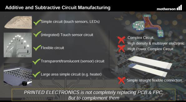
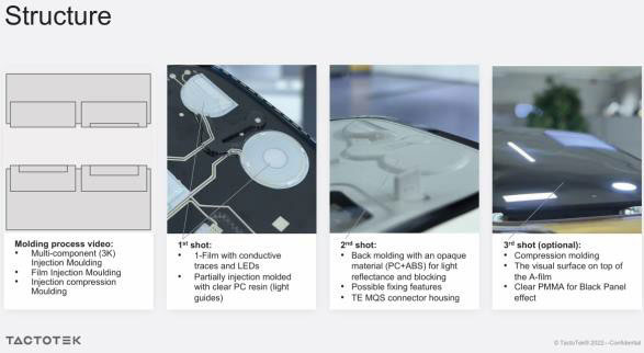
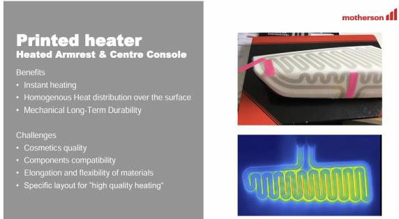
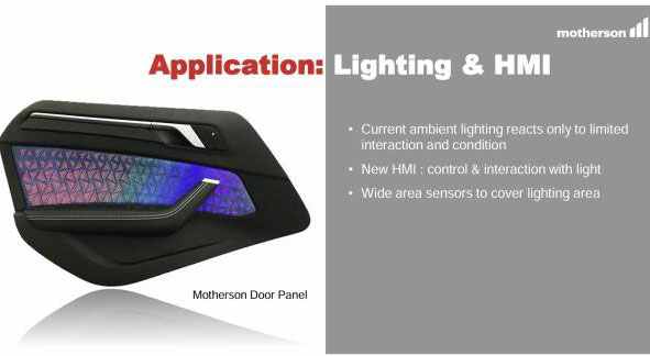
Motherson presented the main challenges for printed electronics and diverse applications.
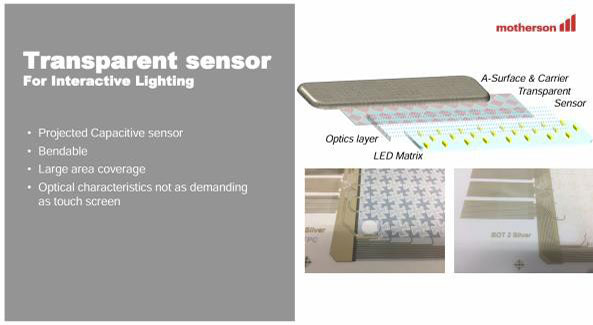
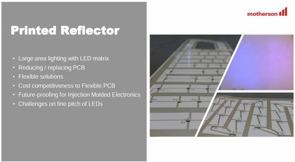
They mentioned good trends for this technology and a bright future, with mainly two points: IPO connector prices have dropped by half during the last five years, and this technology dramatically cuts the CO2 footprint of electronics.

